What’s Under the Black Blob on the Back of LCDs?
Let’s Take a Closer Look
This image shows the detailed CAD work that goes on behind that innocuous black blob of plastic on the back of COB (Chip-On-Board) LCD modules.
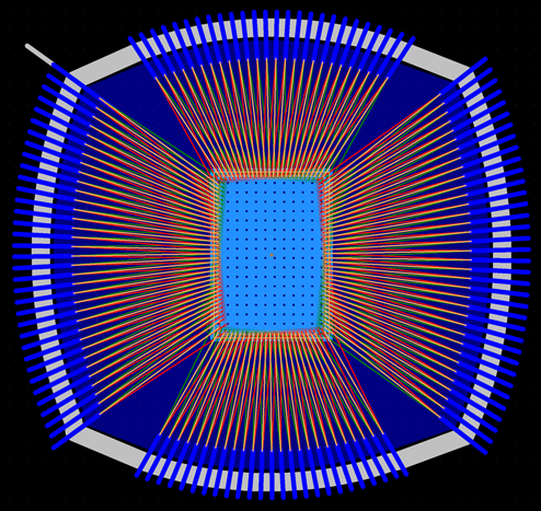
The engineers must analyze the wire bond length and angle to find an optimal solution for placing the pads–while taking into account the range of angles in chip placement that normal production will encounter.
Encased in Clear Resin
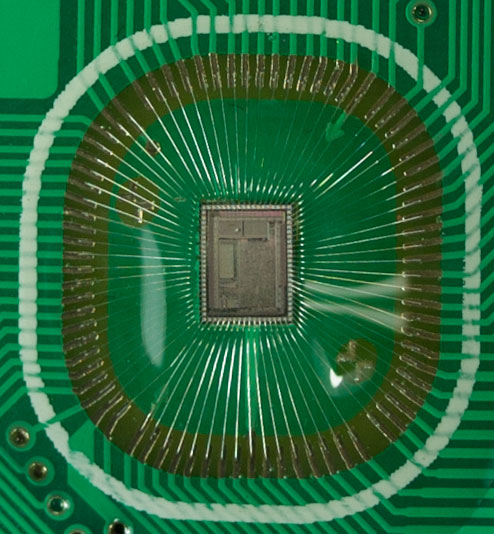
This is a picture of a COB that was encapsulated with clear resin so the wire bonds can be seen. There are well over 100 connections in a typical COB application. Without wire bonding, the modules would have to be much larger.
Why Not Make Them Clear in the First Place?
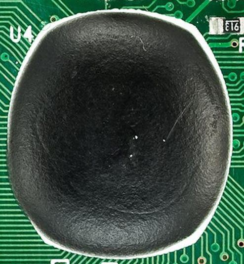
In normal production, a black encapsulant resin is used. The encapsulant protects the chip and the wire bonds.
So why is it black? The chips can be sensitive to light.
Related Trivia: CMOS (Complementary Metal-Oxide Semiconductor) image sensors put this same light sensitivity to good use, and are now found in most digital cameras.
What Crystalfontz LCDs Use This Technology?
Questions?
For any questions about Crystalfontz LCD product lines, what LCD is the best choice for your application, or any other questions (technical or availability), please contact our knowledgeable and friendly support staff via email, phone, or chat.